Nanoscale characterisation at the Institute of Materials
Characterisation of materials at the nanoscale requires techniques that can probe their physicochemical properties with high precision. Our researchers utilize a variety of instruments that provide information on atomic structure, defects, microstructure, strain, and local chemical, electric, optical, and magnetic environment.
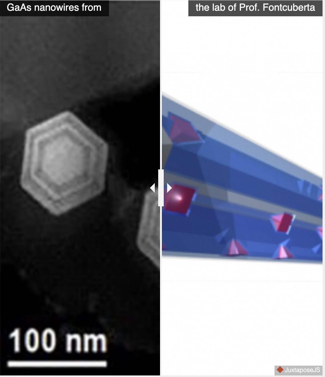
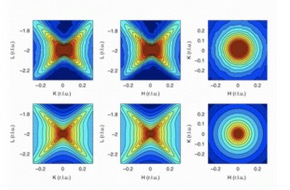
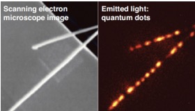
Specialized equipment developed in our Institute is used in combination with the electron microscopy platform at EPFL (CIME) and the x-ray and neutron facilities at PSI. Part of the unique instrumentation also includes a cryo – piezoresponse force microscope (PFM) that allows imaging and quantitative measurements of ferroelectric domain structures at low temperatures, and a quantitative cathodoluminescence (CL) tool for investigating the influence of different types of defects on optical emission of semiconducting materials at the nanometre scale.
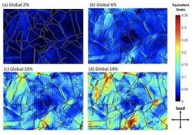
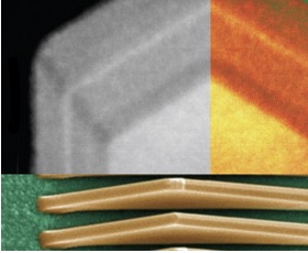
Of particular interest are in situ experiments for probing dynamically the functionality of materials. In situ mechanical testing for strain measurements is being developed to study the slip activity in metastable austenitic stainless steel during deformation. In addition, in situ transmission electron microscopy techniques are being optimized for understanding how the nanomaterial properties are affected by changes in temperature, electric field, and gaseous and/or liquid environment.
Key research themes
- Phase transformations and surface reconstruction of functional oxides
- Degradation of lithium ion batteries by in situ electrochemical methods
- In situ electrocatalysis
- In situ mechanical deformation of steels
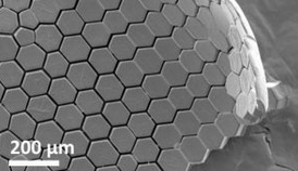
- Self assembly of 2D materials
- Ferroelectric domain structure at various temperatures
- Optical properties of semiconducting materials

